SPE894x
Contents
Overview
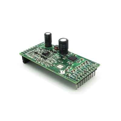
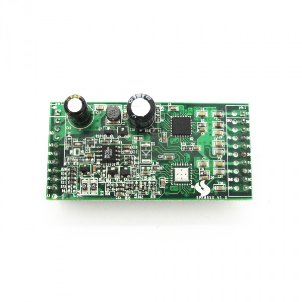
In the PoE scheme, two different types of devices are involved: Power Sourcing Equipment (PSE) and Powered Devices (PD). Compatible with IEEE 802.3af standard, SPE894x is a 4-port channel PSE module for PoE system. It can connect to 4 PD modules at the same time and pass the electric power to them.
SPE89x module supports PoE power management from class 0 to class 4, as well as End-point and Mid-span modes. The Built-in 5A surge TVS tube in PSE output port with the function of short circuit protection can efficiently reduce the damages from short circuit load and surge and provide a stable and safe PoE environment.
Go shopping SPE894x(IM141020001)
Features
- Compatible with IEEE 802.3af standard
- Support 10M/100M/1000M PoE system
- Support End-point and Mid-span modes
- Maximum 600mA current output in each channel
- Support PoE electric power class from 0 to 4
- Under voltage protection, shorted load protection, over current *protection
- Built-in differential mode voltage 1.5kV, 5A peak current *protection in each channel
Application Notes
- IAD
- Multiband WAPs
- RFID system
- POS Terminal
- Industrial automation systems
- IP Phone terminal and iPBXs
- Surveillance System(NVR, IPC)
- Entrance Surveillance System
- 100M/1000M Ethernet gateway/switch/router
- WiMAX ASN/BTS and CPE/ODU system
Electronic Characteristics
| Test condition | Min | Typical | Max | Unit | |
| VEE_ABS | -62 | +0.3 | V | ||
| VEE | IEEE 802.3af (15.4 W) | -57 | -48 | -45 | V |
| VUVLO | VEE from positive to negative | −38 | −36 | V | |
|---|---|---|---|---|---|
| VEE from negative to positive | −33 | −31 | V | ||
| IPORT | Class 0 | 0 | 5 | mA | |
| Class 1 | 8 | 13 | |||
| Class 2 | 16 | 21 | |||
| Class 3 | 25 | 31 | |||
| Class 4 | 35 | 45 | |||
| Over Current | 51 | ||||
| ICUT | Class 0 | 350 | mA | ||
| Class 1 | 91 | ||||
| Class 2 | 160 | ||||
| Class 3 | 350 | ||||
| Class 4 | 600 | ||||
| RON | IPort≤720mA | 0.3 | 0.6 | ||
| 3.3V output | 3.15 | 3.3 | 3.45 | V | |
| DC load | 50 | mA | |||
| T_OP | 0 | 70 | |||
| T_storage | -10 | 70 |
Hardware
Pin Map
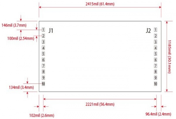
| Number | Name | Description | |
| J1 | 1 | VEE | Input Power(-57~ -45V) |
|---|---|---|---|
| 2 | VEE | Input Power(-57~ -45V) | |
| 3 | GND | ||
| 4 | GND | ||
| 5 | 3.3V | 3.3V output | |
| 6 | SDA | I2C data signal | |
| 7 | SCLK | I2C clock signal | |
| 8 | A0 | Chip Address 0 (1 - access to 3.3V, 0 - Ground ) | |
| 9 | A1 | Chip Address 1 (1 - access to 3.3V, 0 - Ground ) | |
| 10 | RESET | ||
| J2 | 1 | VOUT2 | Class 2 PoE output |
| 2 | GND | ||
| 3 | VOUT3 | Class 3 PoE output | |
| 4 | GND | ||
| 5 | VOUT0 | Class 0 PoE output | |
| 6 | GND | ||
| 7 | VOUT1 | Class 1 PoE output | |
| 8 | GND | ||
| 9 | NC | ||
| 10 | NC |
 Notice

