Difference between revisions of "ITDB06"
m (→Hardware) |
m (→PIN MAP) |
||
| Line 107: | Line 107: | ||
==PIN MAP== | ==PIN MAP== | ||
| + | [[File:IM151229001_ITDB06_pin_map.png|400px]] | ||
| + | |||
| + | {| class="wikitable" | ||
| + | ! scope="col" | No || scope="col" | Pin_Name || scope="col" | Function_Description | ||
| + | |- | ||
| + | | style="text-align:right" | 1 || RST || Reset Module | ||
| + | |- | ||
| + | | style="text-align:right" | 2 || ADC || A / D conversion result. Input voltage range: 0~1V, value range: 0~1024 | ||
| + | |- | ||
| + | | style="text-align:right" | 3 || EN || Chip enable end, high active | ||
| + | |- | ||
| + | | style="text-align:right" | 4 || IO16 || GPIO16; wakeup from deep sleep when connect RESET pin。 | ||
| + | |- | ||
| + | | style="text-align:right" | 5 || IO14 || GPIO14; HSPI_CLK | ||
| + | |- | ||
| + | | style="text-align:right" | 6 || IO12 || GPIO12; HSPI_MISO | ||
| + | |- | ||
| + | | style="text-align:right" | 7 || IO13 || GPIO13; HSPI_MOSI; UART0_CTS | ||
| + | |- | ||
| + | | style="text-align:right" | 8 || VCC || 3.3V | ||
| + | |- | ||
| + | | style="text-align:right" | 9 || CS0 || Chip Select | ||
| + | |- | ||
| + | | style="text-align:right" | 10 || MISO || Master Input Slave Output | ||
| + | |- | ||
| + | | style="text-align:right" | 11 || IO9 || GPIO9 | ||
| + | |- | ||
| + | | style="text-align:right" | 12 || IO10 || GPIO10 | ||
| + | |- | ||
| + | | style="text-align:right" | 13 || MOSI || Master Output Slave Input | ||
| + | |- | ||
| + | | style="text-align:right" | 14 || SCLK || Clock (SCL) | ||
| + | |- | ||
| + | | style="text-align:right" | 15 || GND || GND | ||
| + | |- | ||
| + | | style="text-align:right" | 16 || IO15 || GPIO15; MTDO; HSPICS; UART0_RTS | ||
| + | |- | ||
| + | | style="text-align:right" | 17 || IO2 || GPIO2; UART1_TXD | ||
| + | |- | ||
| + | | style="text-align:right" | 18 || IO0 || GPIO0 | ||
| + | |- | ||
| + | | style="text-align:right" | 19 || IO4 || GPIO4 | ||
| + | |- | ||
| + | | style="text-align:right" | 20 || IO5 || GPIO5 | ||
| + | |- | ||
| + | | style="text-align:right" | 21 || RXD || UART0_RXD; GPIO3 | ||
| + | |- | ||
| + | | style="text-align:right" | 22 || TXD || UART0_TXD; GPIO1 | ||
| + | |} | ||
| + | |||
==Download== | ==Download== | ||
==Useful link== | ==Useful link== | ||
Revision as of 08:42, 16 March 2016
Contents
Overview
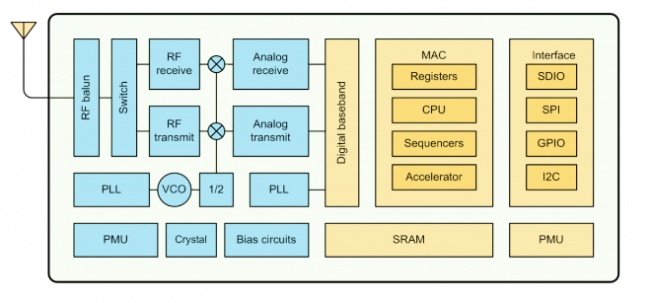
The ITDB06 WiFi Module is a low-cost universal WiFi module that developed and designed by ITEAD. The module integrates industry leading Tensilica L106 ultra-low power 32-bit MCU, 16-bit compact mode, frequency supports 80MHz and 160MHz, supports RTOS, integrates Wi-Fi MAC/ BB/RF/PA/LNA, on-board antenna.
This module supports standard IEEE802.11 b/g/n protocol and complete TCP/IP protocol stack.. It allows users to add Internet of Things (IoT) to devices or to build a separate network controller.
ITDB06 is high performance wireless SOC, it provides maximum usability at the lowest cost, offering unlimited possibilities for adding WiFi functions to other systems.
ITDB06 is a complete and self-contained WiFi network solution that can run independently, it can also be mounted as a slave host MCU operation.
When the module is mounted to application and as the only processor, it can boot directly from the external flash memory. Built-in cache system is provided to increase system performance and reduce memory requirements.
When the wireless network is accessed and undertake WiFi adapter tasks, you can add it to any microcontroller-based design, simply connect SPI/SDIO interface or I2C/UART interface.
The powerful processing and storage capabilities enable it to integrate sensors and other application-specific devices through GPIO, which achieves lowest pre-development and minimal system resources occupation during performing.
This module integrates antenna switch balun and power management converter, thus little external circuitry needed, and the entire solution including the front-end module has reduced the PCB size to a new minimum.
The ITDB06 system leading features include energy saving VoIP quickly switch between sleep/ wake mode, low-power operation self-adaptive radio bias, front-end signal processing capability, troubleshooting and radio systems coexist performance eliminates interference of cellular/Bluetooth/DDR/LVDS/LCD .
Features
- 802.11 b/g/n
- WIFI @2.4 GHz,support WPA/WPA2 safe mode
- Small size 11.5mm*11.5mm
- Built-in 10 bit high accuracy ADC
- Built-in TCP/IP protocol stack
- Built-in switch, balun, LNA, power amplifier and matching network
- Built-in PLL, voltage stabilizer and power management components
- 802.11b mode + 20 dBm output power
- Support antenna diversity
- 10uA deep sleep maintain current, shutdown current is less than 5 uA
- Built-in 32-bit lower power CUP
- SDIO 2.0、SPI、UART
- STBC、1x1 MIMO、2x1 MIMO
- A-MPDU&A-MSDU aggregation and 0.4us guard interval
- Wake-up, connect and transfer data packets in 2 ms
- Standby power consumption: <1.0mW (DTIM3)
- Temp range:-40 ~ 125℃
Specification
| Category | Parameters | Explanation |
|---|---|---|
| Radio parameters | Wireless Standard | 802.11 b/g/n |
| Frequency Range | 2.4G-25G(2400M-2483.5M) | |
| Transmitting power | 802.11b: 20dBm | |
| 802.11g: 17dBm | ||
| 802.11n: 14dBm | ||
| Receiving sensitivity | 802.11b: (11Mbps)-91dbm | |
| 802.11g: (54Mbps)-75dbm | ||
| 802.11n: (MCS7)-72dbm | ||
| Hardware parameters | Data access | UART/HSPI/I2C/I2S/Ir Remote Control |
| GPIO/PWM | ||
| Operating Voltage | 3.0~3.6V(Suggested 3.3V) | |
| Working current | Average: 80mA | |
| Operating temperature | -40°~125° | |
| Storage temperature | Room temperature | |
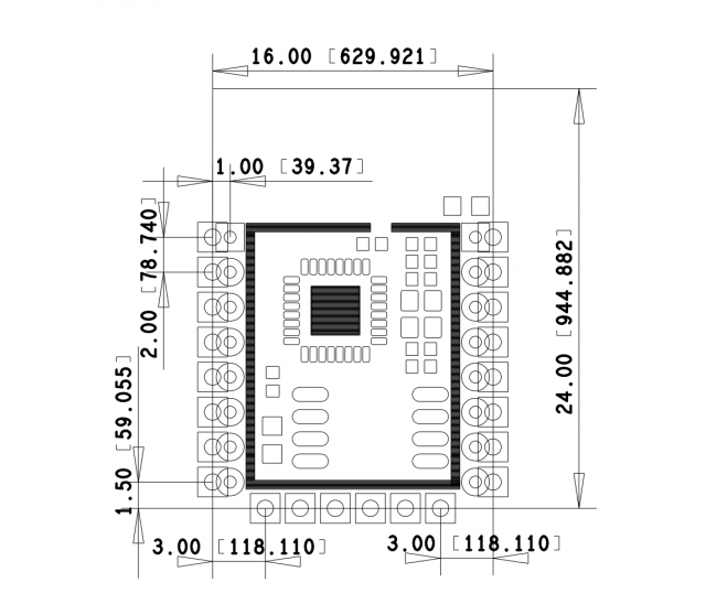
| Size | 16mm*24mm*3mm | |
| Software parameters | Wireless Network Mode | Station/softAP/SoftAP+station |
| Security Mechanism | WPA/WPA2 | |
| Encryption Type | WEP/TKIP/AES | |
| Upgrading firmware | Local serial programming / Cloud Upgrade / Host Download Burn | |
| Network protocol | IPv4, TCP/UDP/HTTP/FTP | |
| User Profiles | AT + instruction set, cloud server, Android/iOS APP |
Electrical Characteristics
| Parameter | Condition | Min | Type | Max | Unit |
|---|---|---|---|---|---|
| Storage temperature | -40 | Room temp. | 125 | ℃ | |
| Max solder temperature | IPC/JEDEC J-STD-020 | 260 | ℃ | ||
| Working voltage | 3.0 | 3.3 | 3.6 | V | |
| I/O VIL/VIH | -0.3/0.75VIO | 0.25VIO/3.6 | V | ||
| I/O VPL/VOH | N/0.8VIO | 0.1VIO/N | V | ||
| I/O Imax | 12 | mA |
Hardware
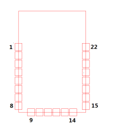
PIN MAP
| No | Pin_Name | Function_Description |
|---|---|---|
| 1 | RST | Reset Module |
| 2 | ADC | A / D conversion result. Input voltage range: 0~1V, value range: 0~1024 |
| 3 | EN | Chip enable end, high active |
| 4 | IO16 | GPIO16; wakeup from deep sleep when connect RESET pin。 |
| 5 | IO14 | GPIO14; HSPI_CLK |
| 6 | IO12 | GPIO12; HSPI_MISO |
| 7 | IO13 | GPIO13; HSPI_MOSI; UART0_CTS |
| 8 | VCC | 3.3V |
| 9 | CS0 | Chip Select |
| 10 | MISO | Master Input Slave Output |
| 11 | IO9 | GPIO9 |
| 12 | IO10 | GPIO10 |
| 13 | MOSI | Master Output Slave Input |
| 14 | SCLK | Clock (SCL) |
| 15 | GND | GND |
| 16 | IO15 | GPIO15; MTDO; HSPICS; UART0_RTS |
| 17 | IO2 | GPIO2; UART1_TXD |
| 18 | IO0 | GPIO0 |
| 19 | IO4 | GPIO4 |
| 20 | IO5 | GPIO5 |
| 21 | RXD | UART0_RXD; GPIO3 |
| 22 | TXD | UART0_TXD; GPIO1 |
 Notice

