Difference between revisions of "Sonoff SV"
m (→Features) |
m |
||
| Line 117: | Line 117: | ||
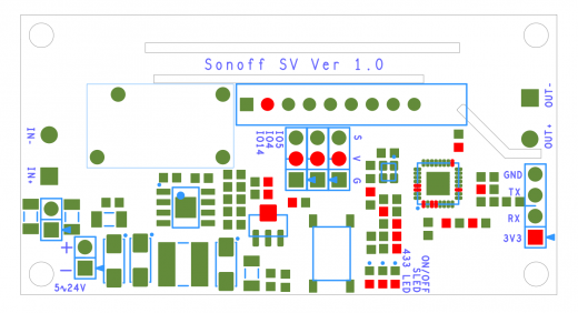
[[File:Sonoff SV hardware.png|520px]] | [[File:Sonoff SV hardware.png|520px]] | ||
| − | == | + | ==Solder Instructions== |
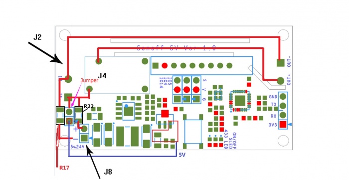
[[File:Sonoff-sv-soldering-guide.jpg|700px]] | [[File:Sonoff-sv-soldering-guide.jpg|700px]] | ||
Revision as of 06:27, 15 March 2016
Contents
Overview
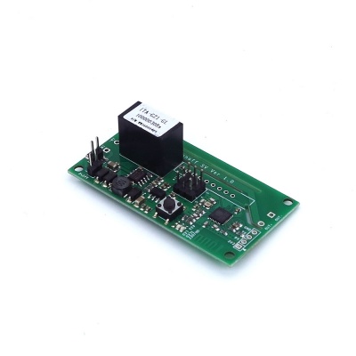
Sonoff SV(safe voltage) is a low power supply Sonoff version,which supports 5-24V power supply. The power separation circuit enables it to control AC or DC power for the connected device, but you need to do some welding to realize this function, please refer to Soldering Instructions below. Sonoff SV has GIPO reserved to support secondary development. This version does not have 433 RF function.
Go shopping Sonoff SV (SKU:IM160220004)
Features
-Support 5~24V power supply.
--Support fast configure SSID and password through APP.
-Support automatic connect to server, register and update status info.
-Support tracking device status and timely remote control through APP.
-Support setting single and repeat timing tasks.
-Reserve GIPO to support secondary development.
WIFI Characteristics
• 802.11 b / g / n
• Built-in Tensilica L106 ultra-low power consumption 32-bit micro-MCU, dominant frequency support 80 MHz and 160 MHz, support RTOS
• Built-in TCP / IP protocol stack
• Built-in TR switch, balun, LNA, power amplifier and matching network
• Built-in PLL, voltage regulator and power supply management components, 802.11b mode +20 dBm output power
• A-MPDU&A-MSDU aggregation and 0.4μs guard interval
• WiFi @ 2.4 GHz, supports WPA / WPA2 safe mode
• Support cloud OTA upgrade
• Support STA / AP / STA + AP mode
• UART, I2C, PWM, GPIO
• Deep sleep maintain current is 10 uA, shutdown current is less than 5 uA
• Wake-up, connect and transfer data packets in 2 ms
• Standby power consumption is less than 1.0 mW (DTIM3)
• Operating temperature range: -40 ℃ - 125 ℃
• Other parameters as follows
| Category | Parameters | Description |
| Wireless Parameter | Wireless standard | 802.11 b/g/n |
| Frequency range | 2.4GHz-2.5GHz (2400M-2483.5M) | |
| Hardware Parameter | Data port | UART/I2C |
| GPIO/PWM | ||
| Operating voltage | 3.0~3.6V(recommend 3.3V) | |
| Operating current | Average: 80mA | |
| Operating temperature | -40°~125° | |
| Storage temperature | Room temperature | |
| Package size | 65mm*34mm*16mm | |
| Software Parameter | Wireless network mode | station/softAP/SoftAP+station |
| Security mechanism | WPA/WPA2 | |
| Encryption type | WEP/TKIP/AES | |
| Firmware upgration | Local serial programming/Cloud Upgrade/Host download programming | |
| Software development | Support secondary development | |
| Network protocols | IPv4, TCP/UDP/HTTP/FTP | |
| User configuration | cloud server, Android/iOS APP |
Specification
| PCB Size | 65X34X1.2mm |
| Interface | UART |
| Indicator LED | WiFi,on/off |
Electrical Characteristics
| Characteristics | Symbol | Min | Typ | Max | Unit |
| Power supply voltage | VDD | 5 | - | 24 | V |
| Operation current for VDD | IDD | - | - | 290 | mA |
Hardware
Solder Instructions
This is a development board, so you can do some soldering to realize different functions.
Work Mode:
Default mode: WIFI circuit and relay circuit adopt the same power supply. You can connect the power supply to J2 or J4. If the input voltage range is within 5-24V, J8 must connect to the jumper; If the input voltage range is within 4-5V, you need to disconnect J8 jumper.
Isolated Mode:
WIFI circuit and relay circuit can be isolated by removing R17 and R22. You will have to power them separately. You can power relay circuit by J2 and power WIFI circuit by J8.
V:3.3V G:GND S:Single
Pin Map
| Pin Index | Pin Name | Description |
| 1 | 3V3 | Chip power |
| 2 | TX | Serial transmit port |
| 3 | RX | Serial receiving port |
| 4 | GND | GND |
| 5 | GPIO4 | I/O |
| 6 | GPIO5 | I/O |
| 7 | GPIO14 | I/O |
 Notice

