Difference between revisions of "IBridge"
From ITEAD Wiki
(→Hardware) |
(→Pins description) |
||
| Line 53: | Line 53: | ||
==Pins description== | ==Pins description== | ||
| + | {| class="wikitable" | ||
| + | |- | ||
| + | | align="center" style="background:#f0f0f0;"|'''Pin''' | ||
| + | | align="center" style="background:#f0f0f0;"|'''Pad Name''' | ||
| + | | align="center" style="background:#f0f0f0;"|'''Type''' | ||
| + | | align="center" style="background:#f0f0f0;"|'''Description''' | ||
| + | |- | ||
| + | | P3||Row2||I||Scan key-board row line 2 | ||
| + | |- | ||
| + | | P4||Row3||I||Scan key-board row line 3 | ||
| + | |- | ||
| + | | P5||Column0||O||Scan key-board column line 0 | ||
| + | |- | ||
| + | | P6||Column1||O||Scan key-board column line 1 | ||
| + | |- | ||
| + | | P7||Column2||O||Scan key-board column line 2 | ||
| + | |- | ||
| + | | P8||Column3||O||Scan key-board column line 3 | ||
| + | |- | ||
| + | | P9||SCK||O||LCD5110 clock | ||
| + | |- | ||
| + | | P10||MO||O||LCD5110 data | ||
| + | |- | ||
| + | | P11||D/Cn||O||LCD5110 data/command select | ||
| + | |- | ||
| + | | P12||RSTn||O||LCD5110 reset | ||
| + | |- | ||
| + | | P13||CSn||O||LCD5110 chip select | ||
| + | |- | ||
| + | | P17||Row0||I||Scan key-board row line 0 | ||
| + | |- | ||
| + | | P18||Row1||I||Scan key-board row line 1 | ||
| + | |- | ||
| + | | P24||GND||G|| | ||
| + | |- | ||
| + | | P25||GND||G|| | ||
| + | |- | ||
| + | | P26||VCC||P|| | ||
| + | |} | ||
===Switch description=== | ===Switch description=== | ||
===Jumper description=== | ===Jumper description=== | ||
==Schematic== | ==Schematic== | ||
Revision as of 08:44, 21 May 2014
Contents
Overview
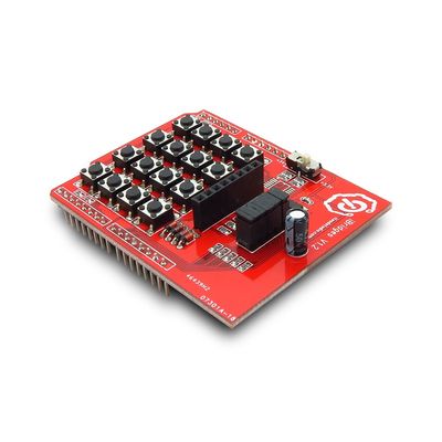
IBridge is a 4X4 key-pad shield with a 5110 Graphic LCD interface.You can plug it on Arduino boards directly, and you can get the small development platform with keypad input and Graphic LCD display.
Specifications
| PCB size | 53.3mm X 68.6mm X 1.6mm |
| Power supply | 5V DC |
| RoSH | Yes |
Electrical Characteristics
| Specification | Min | Type | Max | Unit |
| Power Voltage | 4.5 | 5 | 5.5 | VDC |
| Input Voltage VH (Target Voltage = 3.3V) | 3 | 3.3 | 3.6 | V |
| Input Voltage VH (Target Voltage = 5V) | 4.5 | 5 | 5.5 | |
| Input Voltage VL: | -0.3 | 0 | 0.5 | V |
| Current Consumption(Except Motor Drive Current) | - | 20 | 40 | mA |
Hardware

| Zone | Name | Description |
| 1 | Switch | Set the keypad input level |
| 2 | Jumper | Fix the voltage level that LCD work with |
| 3 | LCD5110 socket | Interface for LCD5110 |
| 4 | Keyboard Zone | 16 buttons in scan keyboard |
Pins description
| Pin | Pad Name | Type | Description |
| P3 | Row2 | I | Scan key-board row line 2 |
| P4 | Row3 | I | Scan key-board row line 3 |
| P5 | Column0 | O | Scan key-board column line 0 |
| P6 | Column1 | O | Scan key-board column line 1 |
| P7 | Column2 | O | Scan key-board column line 2 |
| P8 | Column3 | O | Scan key-board column line 3 |
| P9 | SCK | O | LCD5110 clock |
| P10 | MO | O | LCD5110 data |
| P11 | D/Cn | O | LCD5110 data/command select |
| P12 | RSTn | O | LCD5110 reset |
| P13 | CSn | O | LCD5110 chip select |
| P17 | Row0 | I | Scan key-board row line 0 |
| P18 | Row1 | I | Scan key-board row line 1 |
| P24 | GND | G | |
| P25 | GND | G | |
| P26 | VCC | P |
 Notice