Difference between revisions of "ITDB02-3.2WD"
From ITEAD Wiki
m (→Hardware) |
m (→Features) |
||
| (4 intermediate revisions by 2 users not shown) | |||
| Line 9: | Line 9: | ||
==Features== | ==Features== | ||
| − | |||
* Compatible with UTFT library | * Compatible with UTFT library | ||
* With SD Card Socket | * With SD Card Socket | ||
| Line 20: | Line 19: | ||
| Backlight||4LEDs | | Backlight||4LEDs | ||
|- | |- | ||
| − | | Power supply|| | + | | Power supply||5V |
|- | |- | ||
| Touch Panel||Y | | Touch Panel||Y | ||
| Line 43: | Line 42: | ||
| Power voltage||4.5||5||5.5||VDC | | Power voltage||4.5||5||5.5||VDC | ||
|- | |- | ||
| − | | Input voltage VinH | + | | Input voltage VinH||3||3.3||3.6||V |
| − | + | ||
| − | + | ||
|- | |- | ||
| Input voltage VinL||-0.3||0||0.5||V | | Input voltage VinL||-0.3||0||0.5||V | ||
| Line 148: | Line 145: | ||
[ftp://imall.iteadstudio.com/IM120419006_ITDB02_3.2WD/DS_HX8352-A.pdf Datasheet for HX8352-A] | [ftp://imall.iteadstudio.com/IM120419006_ITDB02_3.2WD/DS_HX8352-A.pdf Datasheet for HX8352-A] | ||
| − | [ | + | [http://www.rinkydinkelectronics.com/library.php?id=51 UTFT library] |
==Useful Links== | ==Useful Links== | ||
| − | [http:// | + | [http://www.rinkydinkelectronics.com/library.php?id=51 by Henning Karlsen <UTFT library>] |
Latest revision as of 02:42, 22 July 2015
Contents
Overview
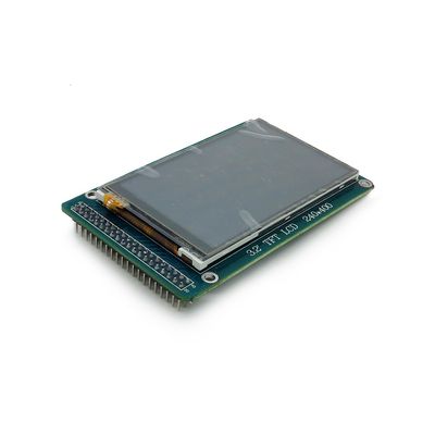
ITDB02-3.2WD module is 3.2" TFT LCD with 65K color 400 x 240 resolutions (16:9 widescreen). The controller of this LCD module is HX8352-A, it supports 16bit data interface with 4 wires control interface. Moreover, this module includes the touch screen and SD card socket.
ITDB02-3.2WD is supported by UTFT Library
Go shopping ITDB02-3.2WD (IM120419006)
Features
- Compatible with UTFT library
- With SD Card Socket
Specifications
| Driver IC | HX8352 |
| Backlight | 4LEDs |
| Power supply | 5V |
| Touch Panel | Y |
| Touch IC | XPT2046 |
| Resolution | 240*400 |
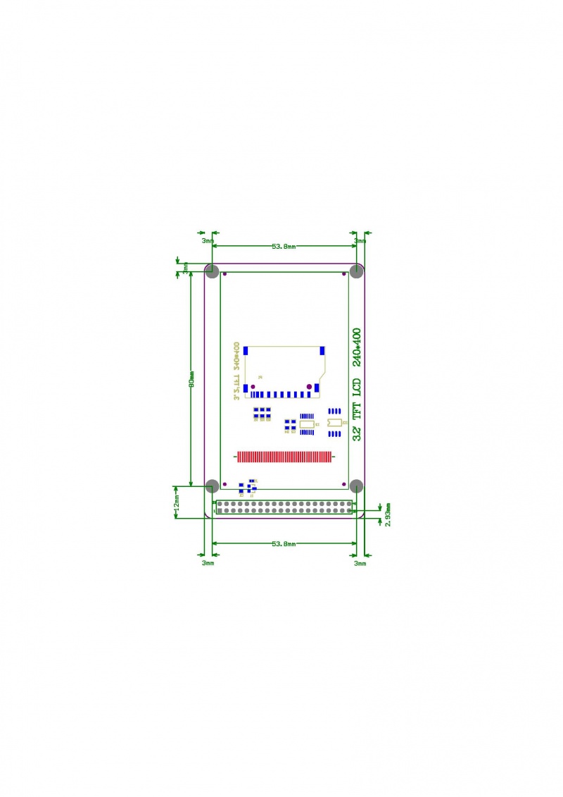
| Size | 95mm*65mm |
Electrical Characteristics
| Parameter | Min. | Typical | Max. | Unit |
| Power voltage | 4.5 | 5 | 5.5 | VDC |
| Input voltage VinH | 3 | 3.3 | 3.6 | V |
| Input voltage VinL | -0.3 | 0 | 0.5 | V |
| Current Consumption | - | 20 | 40 | mA |
Hardware

Pin Map
| Pin | Type* | Description |
| GND | G | Ground |
| VCC | P | 5V Power Supply pin |
| NC | - | No connection |
| RS | I | Data/Command selection |
| WR | I | Write signal enable, low active |
| RD | I | Read signal enable, low active |
| DB8 | I | Data Bus |
| DB9 | I | Data Bus |
| DB10 | I | Data Bus |
| DB11 | I | Data Bus |
| DB12 | I | Data Bus |
| DB13 | I | Data Bus |
| DB14 | I | Data Bus |
| DB15 | I | Data Bus |
| CS | I | Chip Selection,Low level active |
| NC | - | No connection |
| LED | P | Backlight |
| NC | - | No connection |
| DB0 | I | Data Bus |
| DB1 | I | Data Bus |
| DB2 | I | Data Bus |
| DB3 | I | Data Bus |
| DB4 | I | Data Bus |
| DB5 | I | Data Bus |
| DB6 | I | Data Bus |
| DB7 | I | Data Bus |
| T_CLK | I | Touch clock |
| T_CS | I | Touch chip selection |
| T_DIN | I | Touch data input |
| T_BUSY | O | Touch status |
| T_DOUT | O | Touch data output |
| T_IRQ | O | Touch interrupt |
| SD_SO | O | SD MISO |
| SD_SCK | I | SD SCK |
| SD_SI | I | SD MOSI |
| SD_NSS | I | SD NSS |
| NC | - | No connection |
| NC | - | No connection |
 Notice
