Difference between revisions of "Serial Port Bluetooth Module (Master/Slave) : HC-05"
(→Software Features) |
(→Hardware) |
||
| Line 35: | Line 35: | ||
==Hardware== | ==Hardware== | ||
| + | [[File:HC-051.jpg]] | ||
| + | |||
| + | {| class="wikitable" | ||
| + | |- | ||
| + | | align="center" style="background:#f0f0f0;"|'''PIN Name''' | ||
| + | | align="center" style="background:#f0f0f0;"|'''PIN #''' | ||
| + | | align="center" style="background:#f0f0f0;"|'''PAD Type''' | ||
| + | | align="center" style="background:#f0f0f0;"|'''Description''' | ||
| + | | align="center" style="background:#f0f0f0;"|'''Note''' | ||
| + | |- | ||
| + | | GND||13,21,22||VSS||Ground Pot|| | ||
| + | |- | ||
| + | | 3.3 VCC||12||3.3V||Integrated 3.3V(+) supply with On-chip linear regulator output within 3.15-3.3V|| | ||
| + | |- | ||
| + | | AIO0||9||Bi-directional||Programmable input/output line|| | ||
| + | |- | ||
| + | | AIO1||10||Bi-directional||Programmable input/output line|| | ||
| + | |- | ||
| + | | AIO0||23||Bi-directional RX EN||Programmable input/output line, control output for LNA (if fitted)|| | ||
| + | |- | ||
| + | | AIO1||24||Bi-directional TX EN||Programmable input/output line, control output for PA (if fitted)|| | ||
| + | |} | ||
| + | |||
| + | {| class="wikitable" | ||
| + | |- | ||
| + | | align="center" style="background:#f0f0f0;"|'''PIN Name''' | ||
| + | | align="center" style="background:#f0f0f0;"|'''PIN #''' | ||
| + | | align="center" style="background:#f0f0f0;"|'''PAD Type''' | ||
| + | | align="center" style="background:#f0f0f0;"|'''Description''' | ||
| + | | align="center" style="background:#f0f0f0;"|'''Note''' | ||
| + | |- | ||
| + | | PIO2||25||Bi-directional||Programmable input/output line|| | ||
| + | |- | ||
| + | | PIO3||26||Bi-directional||Programmable input/output line|| | ||
| + | |- | ||
| + | | PIO4||27||Bi-directional||Programmable input/output line|| | ||
| + | |- | ||
| + | | PIO5||28||Bi-directional||Programmable input/output line|| | ||
| + | |- | ||
| + | | PIO6||29||Bi-directional||Programmable input/output line|| | ||
| + | |- | ||
| + | | PIO7||30||Bi-directional||Programmable input/output line|| | ||
| + | |- | ||
| + | | PIO8||31||Bi-directional||Programmable input/output line|| | ||
| + | |- | ||
| + | | PIO9||32||Bi-directional||Programmable input/output line|| | ||
| + | |- | ||
| + | | PIO10||33||Bi-directional||Programmable input/output line|| | ||
| + | |- | ||
| + | | PIO11||34||Bi-directional||Programmable input/output line|| | ||
| + | |} | ||
| + | |||
| + | {| class="wikitable" | ||
| + | |- | ||
| + | | align="center" style="background:#f0f0f0;"|'''PIN Name''' | ||
| + | | align="center" style="background:#f0f0f0;"|'''PIN #''' | ||
| + | | align="center" style="background:#f0f0f0;"|'''PAD Type''' | ||
| + | | align="center" style="background:#f0f0f0;"|'''Description''' | ||
| + | | align="center" style="background:#f0f0f0;"|'''Note''' | ||
| + | |- | ||
| + | | RESETB||11||CMOS input with weak internal pull-up||Reset of low.input debouncde so must be low for >5MS to cause a reset|| | ||
| + | |- | ||
| + | | UART_RTS||4||CMOS output, tri-stable with weak internal pull-up||UART request to send, active low|| | ||
| + | |- | ||
| + | | UART_CTS||3||CMOS input with weak internal pull-down||UART clear to send, active low|| | ||
| + | |- | ||
| + | | UART_RX||2||CMOS input with weak internal pull-down||UART Data input|| | ||
| + | |- | ||
| + | | UART_TX||1||CMOS output, tri-stable with weak internal pull-up||UART Data output|| | ||
| + | |- | ||
| + | | SPI_MOSI||17||CMOS input with weak internal pull-down||Serial peripheral interface data input|| | ||
| + | |} | ||
| + | |||
| + | {| class="wikitable" | ||
| + | |- | ||
| + | | align="center" style="background:#f0f0f0;"|'''PIN Name''' | ||
| + | | align="center" style="background:#f0f0f0;"|'''PIN #''' | ||
| + | | align="center" style="background:#f0f0f0;"|'''PAD Type''' | ||
| + | | align="center" style="background:#f0f0f0;"|'''Description''' | ||
| + | | align="center" style="background:#f0f0f0;"|'''Note''' | ||
| + | |- | ||
| + | | SPI_CSB||16||CMOS input with weak internal pull-up||Chip select for serial peripheral interface, active low|| | ||
| + | |- | ||
| + | | SPI_CLK||19||CMOS input with weak internal pull-down||Serial peripheral interface clock|| | ||
| + | |- | ||
| + | | SPI_MISO||18||CMOS input with weak internal pull-down||Serial peripheral interface data output|| | ||
| + | |- | ||
| + | | USB_-||15||Bi-directional|||| | ||
| + | |- | ||
| + | | USB_+||20||Bi-directional|||| | ||
| + | |- | ||
| + | | NC||14|||||| | ||
| + | |- | ||
| + | | PCM_CLK||5||Bi-directional||Synchronous PCM data clock|| | ||
| + | |- | ||
| + | | PCM_OUT||6||CMOS output||Synchronous PCM data output|| | ||
| + | |- | ||
| + | | PCM_IN||7||CMOS input||Synchronous PCM data input|| | ||
| + | |- | ||
| + | | PCM_SYNC||8||Bi-directional||Synchronous PCM data strobe | ||
| + | |} | ||
==AT command Default== | ==AT command Default== | ||
Revision as of 09:28, 28 May 2014
Contents
Overview
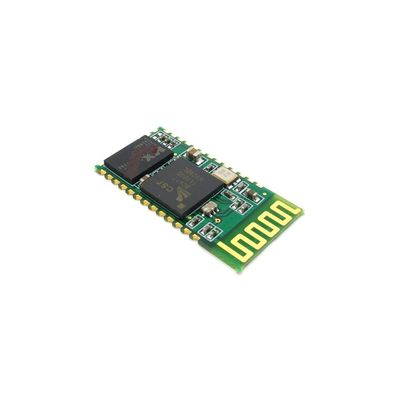
HC-05 module is an easy to use Bluetooth SPP (Serial Port Protocol) module, designed for transparent wireless serial connection setup.
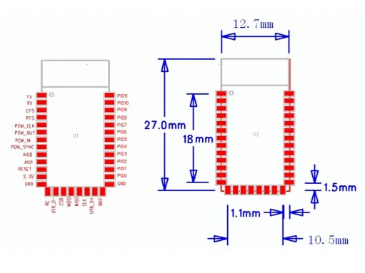
Serial port Bluetooth module is fully qualified Bluetooth V2.0+EDR (Enhanced Data Rate) 3Mbps Modulation with complete 2.4GHz radio transceiver and baseband. It uses CSR Bluecore 04-External single chip Bluetooth system with CMOS technology and with AFH(Adaptive Frequency Hopping Feature). It has the footprint as small as 12.7mmx27mm. Hope it will simplify your overall design/development cycle.
Specifications
Hardware Features
- Typical -80dBm sensitivity
- Up to +4dBm RF transmit power
- Low Power 1.8V Operation ,1.8 to 3.6V I/O
- PIO control
- UART interface with programmable baud rate
- With integrated antenna
- With edge connector
Software Features
- Default Baud rate: 38400, Data bits:8, Stop bit:1,Parity:No parity, Data control: has.
Supported baud rate: 9600,19200,38400,57600,115200,230400,460800.
- Given a rising pulse in PIO0, device will be disconnected.
- Status instruction port PIO1: low-disconnected, high-connected;
- PIO10 and PIO11 can be connected to red and blue led separately. When master and slave
are paired, red and blue led blinks 1time/2s in interval, while disconnected only blue led blinks 2times/s.
- Auto-connect to the last device on power as default.
- Permit pairing device to connect as default.
- Auto-pairing PINCODE:”0000” as default
- Auto-reconnect in 30 min when disconnected as a result of beyond the range of connection.
Hardware
| PIN Name | PIN # | PAD Type | Description | Note |
| GND | 13,21,22 | VSS | Ground Pot | |
| 3.3 VCC | 12 | 3.3V | Integrated 3.3V(+) supply with On-chip linear regulator output within 3.15-3.3V | |
| AIO0 | 9 | Bi-directional | Programmable input/output line | |
| AIO1 | 10 | Bi-directional | Programmable input/output line | |
| AIO0 | 23 | Bi-directional RX EN | Programmable input/output line, control output for LNA (if fitted) | |
| AIO1 | 24 | Bi-directional TX EN | Programmable input/output line, control output for PA (if fitted) |
| PIN Name | PIN # | PAD Type | Description | Note |
| PIO2 | 25 | Bi-directional | Programmable input/output line | |
| PIO3 | 26 | Bi-directional | Programmable input/output line | |
| PIO4 | 27 | Bi-directional | Programmable input/output line | |
| PIO5 | 28 | Bi-directional | Programmable input/output line | |
| PIO6 | 29 | Bi-directional | Programmable input/output line | |
| PIO7 | 30 | Bi-directional | Programmable input/output line | |
| PIO8 | 31 | Bi-directional | Programmable input/output line | |
| PIO9 | 32 | Bi-directional | Programmable input/output line | |
| PIO10 | 33 | Bi-directional | Programmable input/output line | |
| PIO11 | 34 | Bi-directional | Programmable input/output line |
| PIN Name | PIN # | PAD Type | Description | Note |
| RESETB | 11 | CMOS input with weak internal pull-up | Reset of low.input debouncde so must be low for >5MS to cause a reset | |
| UART_RTS | 4 | CMOS output, tri-stable with weak internal pull-up | UART request to send, active low | |
| UART_CTS | 3 | CMOS input with weak internal pull-down | UART clear to send, active low | |
| UART_RX | 2 | CMOS input with weak internal pull-down | UART Data input | |
| UART_TX | 1 | CMOS output, tri-stable with weak internal pull-up | UART Data output | |
| SPI_MOSI | 17 | CMOS input with weak internal pull-down | Serial peripheral interface data input |
| PIN Name | PIN # | PAD Type | Description | Note |
| SPI_CSB | 16 | CMOS input with weak internal pull-up | Chip select for serial peripheral interface, active low | |
| SPI_CLK | 19 | CMOS input with weak internal pull-down | Serial peripheral interface clock | |
| SPI_MISO | 18 | CMOS input with weak internal pull-down | Serial peripheral interface data output | |
| USB_- | 15 | Bi-directional | ||
| USB_+ | 20 | Bi-directional | ||
| NC | 14 | |||
| PCM_CLK | 5 | Bi-directional | Synchronous PCM data clock | |
| PCM_OUT | 6 | CMOS output | Synchronous PCM data output | |
| PCM_IN | 7 | CMOS input | Synchronous PCM data input | |
| PCM_SYNC | 8 | Bi-directional | Synchronous PCM data strobe |
 Notice
